New Manufacturing Process Boosts Military Semiconductor Efficiency
Northrop Grumman image
BALTIMORE – Northrop Grumman is utilizing a new patented transistor technology to improve the speed and efficiency of designing and manufacturing semiconductors for its military customers.
Super-lattice castellated field effect transistors are a circuit technology that use gallium nitride to boost performance levels of semiconductors by implementing “filters, switches and components that are inside of a multi-function sensor” and have very low insertion loss and a smaller footprint, Vern Boyle, vice president of Northrop Grumman’s Microelectronics Center, Mission Systems, said during a recent media event.
The transistors allow future systems to operate equally efficiently with a significant reduction in insertion loss — or the loss of a transmission signal — meaning fewer chips are needed, less data is lost and higher frequency abilities are enabled because of those features, according to the company website.
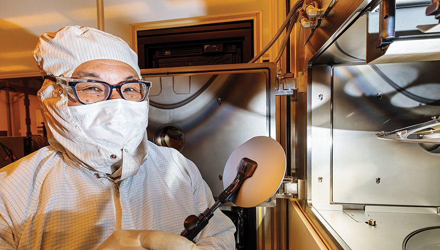
Using this transistor technology “allows us to get the size, the weight, the power and get the performance [of our] semiconductors up,” Boyle said. “This is a computing wafer, so we are building a lot of new technology around superconducting electronics — that is, electronics that [operate] at near zero-degree temperature, very special materials.”
About half of the wafers — or thin slices of semiconductor — that Northrop Grumman processes in its Baltimore, Maryland, facility are designed for multi-function sensing, and the other half are designed for computing. Using the new transistor device improves the efficiency and lowers the overall footprint of manufacturing multi-function semiconductors while maximizing performance and lowering their size and weight, Boyle said.
Northrop Grumman has two internal semiconductor foundries, one in Redondo Beach, California, and the one in Maryland. Each location is focused on different materials and applications: the California foundry mostly manufactures chips for space applications, and the Maryland foundry focuses mainly on airborne applications and advanced computing technology.
The Maryland foundry uses a “low volume, high mix” approach to chip manufacturing. Commercial microchip fabrication plants, or fabs, make “millions of chips,” Boyle said.
“We need lower volume, purpose-built chips. … The high mix refers to the variety of materials that we work with,” he said. “A commercial fab might make one or two products. We make 90 products across our fabs. They might work with a small mix of materials. We work with a high mix because we’re driving those 90 products into over 60 different programs and systems across Northrop Grumman.”
When it comes to designing and manufacturing products for the military — especially electronics — the government’s unique and specific requirements must be addressed all the way down to the semiconductor level, Boyle said.
One application is for radars with wide bandwidths and high frequencies, he said. “When you look at the front end of a tactical fighter, there’s not a lot of space, so size, weight and power become really important. And how we build and design those custom chips drives the performance of the mission systems that they go into.”
Northrop Grumman is using digital tools and spurring a digital transformation on the semiconductor level through the design process and product lines, Boyle said.
The company uses digital modeling and twins to “design the chip, understand how it integrates up to the next packaging level up onto the board level, up into the chassis level, so that when [we] make these custom build parts, we can get it right the first time, and that reduces the cost and reduces the schedule,” he said.
On the production side, the company integrates product data into a digital thread and uses automation and robots to ensure improved assembly line efficiency.
“All the data and all the information that tracks that [chip], from the wafer to the aircraft, is all part of that digital transformation thread,” Boyle said. “[If] you’re running a test, and you find something isn’t working, and it’s isolated down into the electronics, we can trace it all the way back to the process that was used — the day, the hour it was manufactured. … We can do that very fast because all that data is integrated as part of the digital thread.” ND
Topics: Cyber, Defense Department


Discussion about this post