


Researchers have utilized AI to uncover new insights into dislocations in polycrystalline materials, challenging existing scientific models and paving the way for enhanced material performance in electronics and solar cells. Credit: SciTechDaily.com
Scientists at 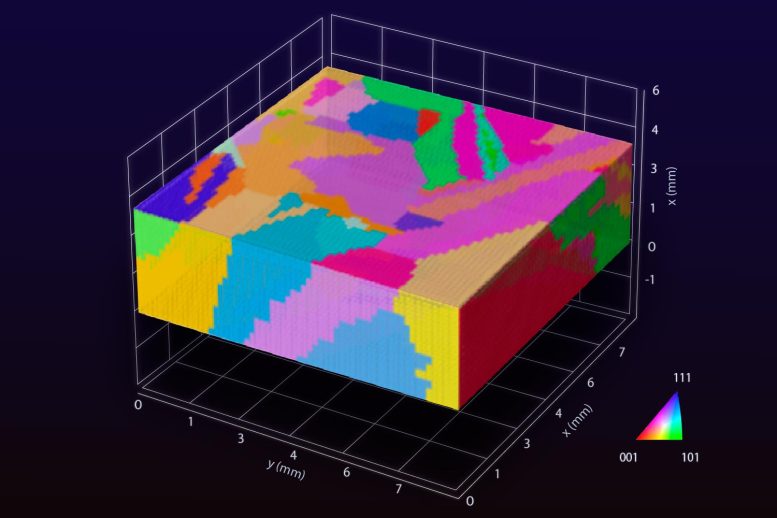
Researchers used 3D models created by AI to understand complex polycrystalline materials that are used in our everyday electronic devices. Credit: Kenta Yamakoshi
AI-Driven Discovery
A team of researchers at Nagoya University, led by Professor Noritaka Usami and including Lecturer Tatsuya Yokoi and Associate Professor Hiroaki Kudo and collaborators, used a new AI to analyze image data of a material widely used in solar panels, called polycrystalline silicon. The AI created a 3D model in virtual space, helping the team to identify the areas where dislocation clusters were affecting the material’s performance.
After identifying the areas of the dislocation clusters, the researchers used electron microscopy and theoretical calculations to understand how these areas formed. They revealed stress distribution in the crystal lattice and found staircase-like structures at the boundaries between the crystal grains. These structures appear to cause dislocations during crystal growth. “We found a special nanostructure in the crystals associated with dislocations in polycrystalline structures,” Usami said.
Implications for Crystal Growth Science
Along with its practical implications, this study may have important implications for the science of crystal growth and deformation as well. The Haasen-Alexander-Sumino (HAS) model is an influential theoretical framework used to understand the behavior of dislocations in materials. But Usami believes that they have discovered dislocations that the Haasen-Alexander-Sumino model missed.
New Insights Into Atom Arrangement
Another surprise was to follow soon after, as when the team calculated the arrangement of the atoms in these structures, they found unexpectedly large tensile bond strains along the edge of the staircase-like structures that triggered dislocation generation.
As explained by Usami, “As experts who have been studying this for years, we were amazed and excited to finally see proof of the presence of dislocations in these structures. It suggests that we can control the formation of dislocation clusters by controlling the direction in which the boundary spreads.”
Conclusion and Future Implications
“By extracting and analyzing the
” data-gt-translate-attributes=”[{“attribute”:”data-cmtooltip”, “format”:”html”}]” tabindex=”0″ role=”link”>semiconductors. Polycrystalline materials are widely used in society, and the improved performance of these materials has the potential to revolutionize society.”
Reference: “Multicrystalline Informatics Applied to Multicrystalline Silicon for Unraveling the Microscopic Root Cause of Dislocation Generation” by Kenta Yamakoshi, Yutaka Ohno, Kentaro Kutsukake, Takuto Kojima, Tatsuya Yokoi, Hideto Yoshida, Hiroyuki Tanaka, Xin Liu, Hiroaki Kudo and Noritaka Usami, 2 December 2023, Advanced Materials.
DOI: 10.1002/adma.202308599


