

Researchers at Rice University and UC Berkeley have discovered that antiferroelectrics, particularly lead zirconate, demonstrate significantly higher electromechanical responses compared to traditional piezoelectric materials when miniaturized. This breakthrough could lead to the development of more efficient and powerful miniaturized electronic devices.
A study by Rice University identifies a high-performance alternative to traditional ferroelectrics.
Lighting a gas grill, getting an ultrasound, using an ultrasonic toothbrush ⎯ these actions involve the use of materials that can translate an electric voltage into a change in shape and vice versa.
Known as piezoelectricity, the ability to trade between mechanical stress and electric charge can be harnessed widely in capacitors, actuators, transducers, and sensors like accelerometers and gyroscopes for next-generation electronics. However, integrating these materials into miniaturized systems has been difficult due to the tendency of electromechanically active materials to ⎯ at the submicrometer scale, when the thickness is just a few millionths of an inch ⎯ get “clamped” down by the material they are attached to, which significantly dials down their performance.
Rice University researchers and collaborators at the 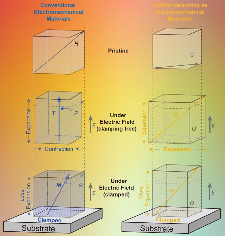
Performance of conventional electromechanical materials versus antiferroelectrics. Credit: Schematic courtesy of Hao Pan
“We’ve been using piezoelectric materials for decades,” said Rice materials scientist Lane Martin, who is the corresponding author on the study. “Recently there has been a strong motivation to further integrate these materials into new types of devices that are very small ⎯ as you would want to do for, say, a microchip that goes inside your phone or computer. The problem is that these materials are typically just less usable at these small scales.”
According to current industry standards, a material is considered to have very good electromechanical performance if it can undergo a 1% change in shape ⎯ or strain ⎯ in response to an electric field. For an object that measures 100 inches in length, for instance, getting 1 inch longer or shorter represents 1% strain.
“From a materials science perspective, this is a significant response, since most hard materials can only change by a fraction of a percent,” said Martin, the Robert A. Welch Professor, professor of materials science and nanoengineering and director of the Rice Advanced Materials Institute.
Clamping Effects on Piezoelectrics
When conventional piezoelectric materials are scaled down to systems less than a micrometer (1,000 nanometers) in size, their performance generally deteriorates significantly due to the interference of the substrate, which dampens their ability to change shape in response to electric field or, conversely, to generate voltage in response to a change in shape.

Lane Martin is Rice University’s Robert A. Welch Professor, professor of materials science and nanoengineering, and director of the Rice Advanced Materials Institute. Credit: Jeff Fitlow/Rice University
According to Martin, if electromechanical performance were rated on a scale of 1-10 ⎯ where 1 is the lowest performance and 10 is the industry standard of 1% strain ⎯ then clamping is typically expected to bring conventional piezoelectrics’ electromechanical response down from a 10 to the 1-4 range.
“To understand how clamping impacts motion, first picture being in a middle seat on an airplane with no one on either side of you ⎯ you’d be free to adjust your position if you get uncomfortable, overheated, etc.,” Martin said. “Now picture the same scenario, except now you’re seated between two huge offensive linemen from Rice’s football team. You’d be ‘clamped’ between them such that you really couldn’t meaningfully adjust your position in response to a stimulus.”
The researchers wanted to understand how very thin films of antiferroelectrics ⎯ a class of materials that remained understudied until recently due to a lack of access to “model” versions of the materials and to their complex structure and properties ⎯ changed their shape in response to voltage and whether they were likewise susceptible to clamping.
First, they grew thin films of the model antiferroelectric material PbZrO 3 with very careful control of the material thickness, quality and orientation. Next, they performed an array of electrical and electromechanical measurements to quantify the responses of the thin films to applied electric voltage.
“We found the response was considerably larger in the thin films of antiferroelectric material than what is achieved in similar geometries of traditional materials,” said Hao Pan, a postdoctoral researcher in Martin’s research group and lead author on the study.
Measuring shape change at such small scales was not an easy feat. In fact, optimizing the measurement setup required so much labor the researchers documented the process in a separate publication.
“With the perfected measurement setup, we can get a resolution of two picometers ⎯ that’s about a thousandth of a nanometer,” Pan said. “But just showing that a shape change happened doesn’t mean we understand what’s going on, so we had to explain it. This was one of the first studies to reveal the mechanisms behind this high performance.”
Observation of Material Changes and Implications
With support from their collaborators at the Massachusetts Institute of Technology, the researchers used a state-of-the-art transmission electron microscope to observe the DOI: 10.1038/s41563-024-01907-y
The research was supported by the U.S. Department of Energy (DE-AC02-05-CH11231, DE-SC-0012375), the Army/ARL (W911NF-19-2-0119), the Army Research Office (W911NF-21-1-0118, W911NF-21-1-0126), the SRC-JUMP ASCENT center, the Department of Defense (FA9550-18-1-0480), the National Science Foundation (1752814) and the National Energy Research Scientific Computing Center. The content of this press release is solely the responsibility of the authors and does not necessarily represent the official views of the funding organizations.
